Design Methodology
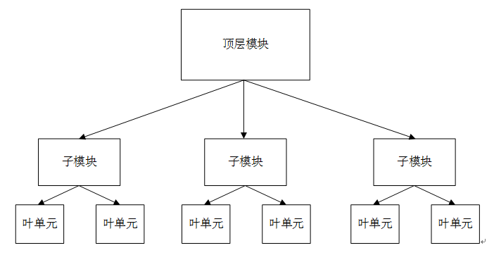
Verilog design mostly adopts a top-down design methodology. That is, first define the functions of the top-level module, then analyze the necessary sub-modules required to form the top-level module; then further decompose and design each module until reaching the bottom-level functional blocks that cannot be further decomposed. In this way, a large system can be refined into multiple small systems, and allocated to more designers in terms of time and workload, thereby improving design speed and shortening the development cycle.
Design Flow
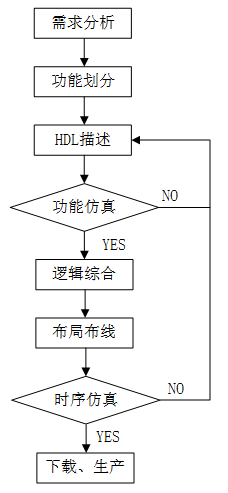
The Verilog design flow generally includes the following steps:
Requirements Analysis
Staff need to analyze and understand the functional requirements proposed by the user, make an overall plan for the circuit system, form detailed technical specifications, and determine a preliminary solution. For example, to design an electronic screen, it is necessary to consider the power supply method, operating frequency, product size, cost, power consumption, etc., and whether the circuit implementation uses ASIC or FPGA/CPLD devices.
Functional Partitioning
After correctly analyzing the user's circuit requirements, the overall design of the logic function can be carried out, designing the functionality, interfaces, and overall structure of the entire circuit, considering the division of functional modules and design ideas, the interfaces and timing of each sub-module (including interface timing and internal signal timing), etc., and reasonably assigning sub-module design tasks to project team members.
Text Description
You can use any text editor or a dedicated HDL editing environment to design and model the required digital circuit, and save it as.vfile.
Functional Simulation (Pre-simulation)
Compile the modeling file, perform functional simulation verification on the model circuit, and find and correct design errors.
The simulation verification at this time does not consider timing factors such as signal delays; it only verifies logical correctness.
Logic Synthesis
Synthesis is the process of converting the high-level description of the design (Verilog modeling) into a gate-level netlist based on the standard cell library and specific design constraints. The purpose of logic synthesis is to produce the gate-level structure of the physical circuit, perform a certain degree of optimization in logic and timing, seek a balance between logic, area, and power consumption, and enhance the testability of the circuit.
However, not all Verilog statements can be synthesized into logic cells, such as delay statements.
Place and Route
According to the netlist and constraint files generated by logic synthesis, place and route the gate-level circuit using the various basic standard cell libraries provided by the manufacturer. At this point, the digital circuit designed in Verilog has been realized as a digital circuit composed of standard cell libraries.
Timing Simulation (Post-simulation)
After place and route, the circuit model already contains delay information. Use the precise parameters obtained in place and route to verify the circuit's timing with simulation software. Differences in cell devices and place-and-route schemes can affect the circuit's timing, and in severe cases, errors may occur. After errors occur, it may be necessary to modify the RTL (Register Transfer Level description, i.e., the initial Verilog description) again and repeat the subsequent steps. This process may be repeated multiple times until all errors are completely eliminated.
FPGA/CPLD Download or ASIC Manufacturing
After completing all the above steps, you can use development tools to download the target file of the designed digital circuit into the FPGA/CPLD chip, and then debug and verify it on the circuit board.
If it is to be implemented on an ASIC, the chip needs to be manufactured. Generally, during chip manufacturing, logic function verification also needs to be performed on an FPGA board first.