The following table shows the percentage of power reduction achievable at various levels of digital design. After the RTL level, the amount of power reduction is already very limited.
| Design level | Improvement degree |
|---|---|
| System level | 50% ~ 90% |
| RTL level | 20% ~ 50% |
| Gate level | 10% ~ 15% |
| Transistor level | 5% ~ 10% |
| Layout level | < 5% |
As a pseudo-coder who writes Verilog, one can participate in some system-level power reduction work, but the focus should be on reducing power at the RTL level.
The following is divided into 2 sections to introduce common methods for reducing power at the RTL level.
Parallelism and Pipelining
For a functional module, it can be implemented in a parallel manner or in a pipelined manner. Both methods trade resources for speed. Flexible use of these two methods in certain situations can reduce power consumption.
Parallel processing
Parallel processing can handle multiple execution statements simultaneously, making execution more efficient. Therefore, under conditions that meet work requirements, adopting parallel processing can reduce the system operating frequency and lower power consumption.
For example, the code descriptions for using 1 multiplier and 2 multipliers (parallel) to implement 4 data multiply-accumulate operations are as follows:
Example
//1 multiplier, high speed
module mul1_hs
(
input clk , //200MHz
input rstn ,
input en ,
input [3:0] mul1 , //data in
input [3:0] mul2 , //data in
output dout_en ,
output [8:0] dout
);
reg flag ;
reg en_r ;
always @(posedge clk or negedge rstn) begin
if (!rstn) begin
flag <= 1'b0 ;
en_r <= 1'b0 ;
end
else if (en) begin
flag <= ~flag ;
en_r <= 1'b1 ;
end
else begin
flag <= 1'b0 ;
en_r <= 1'b0 ;
end
end
wire [7:0] result = mul1 * mul2 ;
// data output en
reg [7:0] res1_r, res2_r ;
always @(posedge clk or negedge rstn) begin
if (!rstn) begin
res1_r <= 'b0 ;
res2_r <= 'b0 ;
end
else if (en & !flag) begin
res1_r <= result ;
end
else if (en & flag) begin
res2_r <= result ;
end
end
assign dout_en = en_r & !flag ;
assign dout = res1_r + res2_r ;
endmodule
//===========================================
// 2 multiplier2, low speed
module mul2_ls
(
input clk , //100MHz
input rstn ,
input en ,
input [3:0] mul1 , //data in
input [3:0] mul2 , //data in
input [3:0] mul3 , //data in
input [3:0] mul4 , //data in
output dout_en,
output [8:0] dout
);
wire [7:0] result1 = mul1 * mul2 ;
wire [7:0] result2 = mul3 * mul4 ;
//en delay
reg en_r ;
always @(posedge clk or negedge rstn) begin
if (!rstn) begin
en_r <= 1'b0 ;
end
else begin
en_r <= en ;
end
end
// data output en
reg [7:0] res1_r, res2_r ;
always @(posedge clk or negedge rstn) begin
if (!rstn) begin
res1_r <= 'b0 ;
res2_r <= 'b0 ;
end
else if (en) begin
res1_r <= result1 ;
res2_r <= result2 ;
end
end
assign dout = res1_r + res2_r ;
assign dout_en = en_r ;
endmodule
The testbench is described as follows.
Example
module test ;
reg rstn ;
//mul1_hs
reg hs_clk;
reg hs_en ;
reg [3:0] hs_mul1 ;
reg [3:0] hs_mul2 ;
wire hs_dout_en ;
wire [8:0] hs_dout ;
//mul1_ls
reg ls_clk = 0;
reg ls_en ;
reg [3:0] ls_mul1 ;
reg [3:0] ls_mul2 ;
reg [3:0] ls_mul3 ;
reg [3:0] ls_mul4 ;
wire ls_dout_en ;
wire [8:0] ls_dout ;
//clock generating
real CYCLE_200MHz = 5 ; //
always begin
hs_clk = 0 ; #(CYCLE_200MHz/2) ;
hs_clk = 1 ; #(CYCLE_200MHz/2) ;
end
always begin
@(posedge hs_clk) ls_clk = ~ls_clk ;
end
//reset generating
initial begin
rstn = 1'b0 ;
#8 rstn = 1'b1 ;
end
//motivation
initial begin
hs_mul1 = 0 ;
hs_mul2 = 16 ;
hs_en = 0 ;
#103 ;
repeat(12) begin
@(negedge hs_clk) ;
hs_en = 1 ;
hs_mul1 = hs_mul1 + 1;
hs_mul2 = hs_mul2 - 1;
end
hs_en = 0 ;
end
initial begin
ls_mul1 = 1 ;
ls_mul2 = 15 ;
ls_mul3 = 2 ;
ls_mul4 = 14 ;
ls_en = 0 ;
#103 ;
@(negedge ls_clk) ls_en = 1;
repeat(5) begin
@(negedge ls_clk) ;
ls_mul1 = ls_mul1 + 2;
ls_mul2 = ls_mul2 - 2;
ls_mul3 = ls_mul3 + 2;
ls_mul4 = ls_mul4 - 2;
end
ls_en = 0 ;
end
//module instantiation
mul1_hs u_mul1_hs
(
.clk (hs_clk),
.rstn (rstn),
.en (hs_en),
.mul1 (hs_mul1),
.mul2 (hs_mul2),
.dout (hs_dout),
.dout_en (hs_dout_en)
);
mul2_ls u_mul2_ls
(
.clk (ls_clk),
.rstn (rstn),
.en (ls_en),
.mul1 (ls_mul1),
.mul2 (ls_mul2),
.mul3 (ls_mul3),
.mul4 (ls_mul4),
.dout (ls_dout),
.dout_en (ls_dout_en)
);
//simulation finish
always begin
#100;
if ($time >= 1000) begin
#1 ;
$finish ;
end
end
endmodule
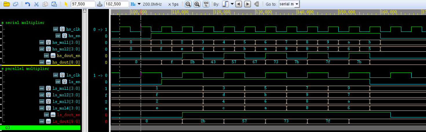
The simulation results are as follows.
It can be seen from the figure that the two implementation methods produce the same output results, but the parallel processing method reduces the operating frequency by half, so power consumption will decrease, while the design area will also increase.
Pipelining
In"Verilog Tutorial"It was described that a continuously working N-stage pipeline design improves efficiency by a factor of about N. Like parallel design, when using pipeline design, the operating frequency can also be appropriately reduced to lower power consumption.
From another perspective, a pipeline design can divide a long combinational path into N pipeline stages. The path length is shortened to 1/N of the original path length. At this time, if the clock frequency remains unchanged, within one cycle, only the capacitance C/N needs to be charged and discharged, rather than the original capacitance C. Therefore, under the same frequency requirement, a lower power supply voltage can be used to drive the system, reducing power consumption.
Suppose in a design, the critical path is a 32-bit by 32-bit multiplier. The overall capacitance of this multiplier is C, and the operating voltage is V.
Without pipelining, to achieve this operating frequency, the operating voltage should be V.
When using a two-stage pipeline, the path is divided into two parts. For each part, the overall capacitance becomes C/2. To achieve the original operating frequency, the operating voltage can be reduced to βV (β<1). The power consumption of the entire system is reduced to β^2 of the original.
For specific pipeline design methods, please refer to"Verilog Tutorial"in the chapter"6.7 Verilog Pipeline"section.
Resource Sharing and State Encoding
Resource sharing
When some identical operation logic is used in multiple places in a design, resource sharing can be used to avoid duplication of multiple operation logic blocks and reduce resource consumption.
For example, for a comparison logic, the code description without resource sharing is as follows:
Example
case (mode) :
3'b000: result = 1'b1 ;
3'b001: result = 1'b0 ;
3'b010: result = value1 == value2 ;
3'b011: result = value1 != value2 ;
3'b100: result = value1 > value2 ;
3'b101: result = value1 < value2 ;
3'b110: result = value1 >= value2 ;
3'b111: result = value1 <= value2 ;
endcase
end
The above code is optimized and described as follows:
wire equal_con = value1 == value2 ;
wire great_con = value1 > value2 ;
always @(*) begin
case (mode) :
3'b000: result = 1'b1 ;
3'b001: result = 1'b0 ;
3'b010: result = equal_con ;
3'b011: result = equal_con ;
3'b100: result = great_con ;
3'b101: result = !great_con && !equal_con ;
3'b110: result = great_con && equal_con ;
3'b111: result = !great_con ;
endcase
end
When the first method is synthesized, if the compiler optimization is not done well, 6 comparators may be needed. The second resource sharing method only needs 2 comparators to complete the same logic function, thus reducing power consumption to a certain extent.
State encoding
For some frequently changing signals, the toggle rate is relatively high and power consumption is relatively large. State encoding can be used to reduce switching activity and lower power consumption.
For example, when a high-speed counter operates, using Gray code instead of binary encoding causes only 1 bit of data to toggle at any time, reducing the toggle rate and thereby lowering power consumption.
For example, when designing a state machine, if the state encoding before and after a state transition differs by only 1 bit, the toggle rate will also be reduced.
Operand Isolation
Operand isolation principle: If the output of a data path is useless during a certain period of time, setting the input to a fixed value prevents switching in the data path, thereby reducing power consumption.
A multiplier circuit diagram is shown below.
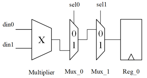
When sel0 = 0 or sel1 = 1, the output of the multiplier cannot reach the input of the register through the two Muxes. That is, the register cannot store the current multiplier result, so this multiplication operation is unnecessary. Under such conditions, operand isolation can be used to keep the multiplier inactive and static, which also saves power.
An optimization of the above circuit is shown in the following figure.
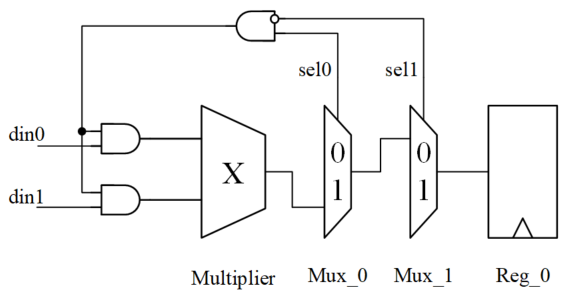
After operand isolation, when sel0 = 0 or sel1 = 1, the multiplier input is always 0, no signal toggling occurs, and the multiplier does not perform extra invalid work, so power consumption is reduced.
Generally speaking, operand isolation occurs during logic synthesis. This process is often manually configurable and can be automatically recognized by the compiler. Of course, good coding style that considers these aspects thoroughly when writing RTL circuits is more conducive to implementing operand isolation and thus reducing power consumption.
When the multiplier does not use operand isolation, the Verilog code description is as follows:
Example
module oper_isolation1
(
input clk , //100MHz
input [1:0] sel ,
input [3:0] din1 , //data in
input [3:0] din2 , //data in
output reg [7:0] dout
);
reg [7:0] res ;
always @(*) begin
res = din1 * din2 ;
end
always @(posedge clk) begin
if (sel == 2'b01) begin
dout <= res ;
end
end
endmodule
When the multiplier uses operand isolation, the Verilog code description is as follows:
Example
module oper_isolation2
(
input clk , //100MHz
input [1:0] sel ,
input [3:0] din1 , //data in
input [3:0] din2 , //data in
output reg [7:0] dout
);
wire [3:0] mul1 = sel == 2'b01 ? din1 : 0 ;
wire [3:0] mul2 = sel == 2'b01 ? din2 : 0 ;
reg [7:0] res ;
always @(*) begin
res = mul1 * mul2 ;
end
always @(posedge clk) begin
if (sel == 2'b01) begin
dout <= res ;
end
end
endmodule
Source Code Download for This Chapter
Download